
IBM's Revolutionary 0.7 nm Chip: A Leap Forward in Technology
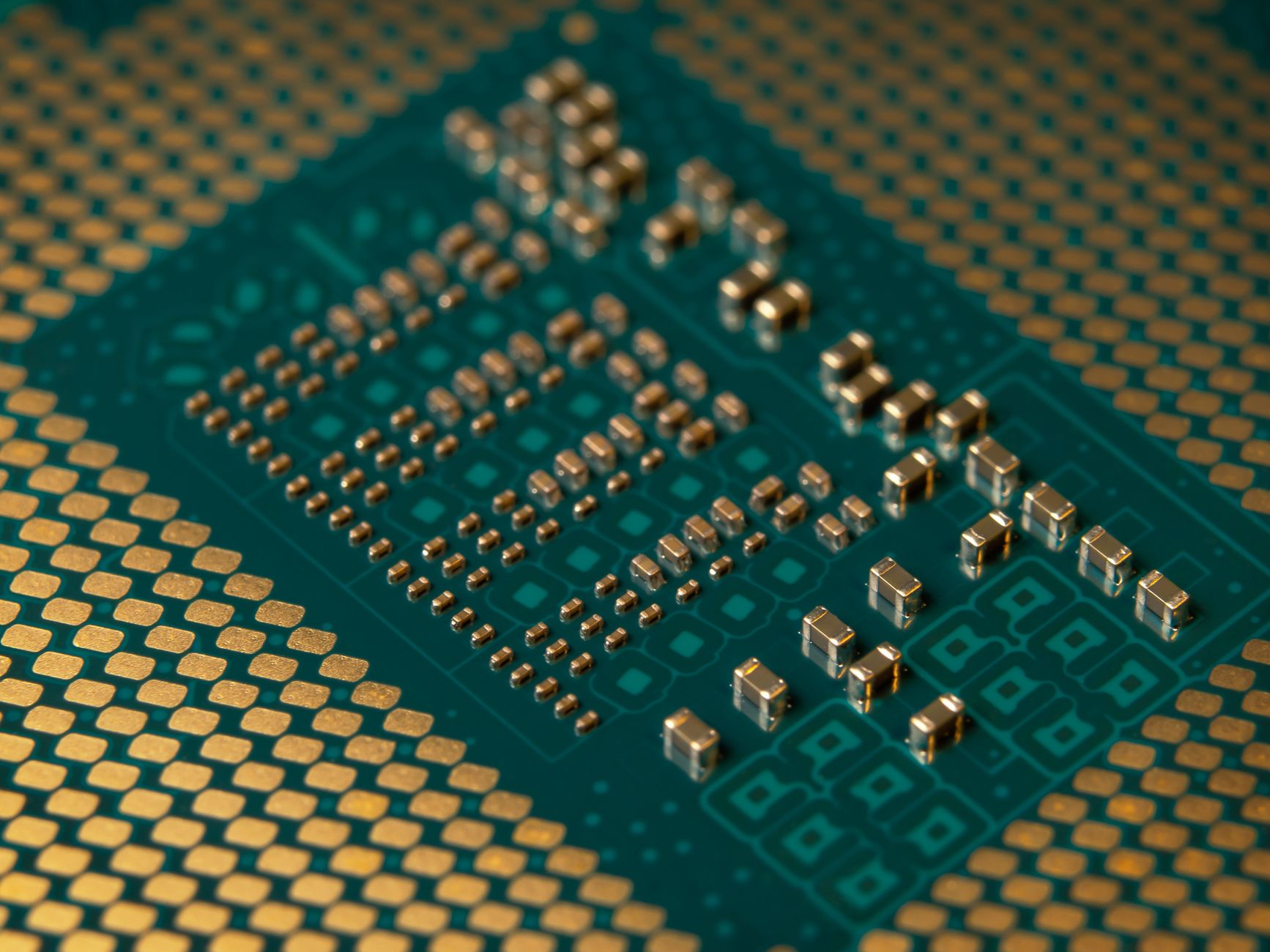
In a world where technological marvels often come cloaked in hyperbole, IBM's latest offering might just live up to its monumental billing. The American tech giant has unveiled the world's first sub-1 nanometer chip technology, a feat that redefines the boundaries of semiconductor engineering.
The 0.7 nanometer chip, roughly the size of a fingernail, manages to pack in a staggering 100 billion transistors. For those who flinch at the mention of transistors, these are the tiny switches that form the bedrock of computer processing. In practical terms, this means a chip that offers 50% more performance or 70% better energy efficiency compared to its predecessors.
A Technological Breakthrough
This innovation, as IBM claims, is not merely about packing more power into smaller spaces. It represents a shift in the architecture of chip design, with transistors now stacked vertically in two layers. This novel approach effectively doubles the density of transistors, setting a new benchmark for efficiency and performance.
Such advancements have profound implications, particularly for artificial intelligence and high-performance computing applications. With AI systems demanding ever-more computational heft, IBM's breakthrough could dramatically enhance the speed and efficiency of data processing, enabling more complex algorithms to be run in shorter timescales.
Looking Ahead
IBM's pioneering chip technology is not expected to remain an academic exercise for long. The company anticipates that this technology could enter production within five years, potentially revolutionising industries dependent on high computing power.
While the technical details might be lost on the average consumer, the implications are clear: faster, more energy-efficient devices that could reshape our digital lives. As the tech world watches closely, IBM's innovation might indeed signal a new era in computing technology.