The Unexpected Crucial Role of Advanced Chip Packaging in A.I.
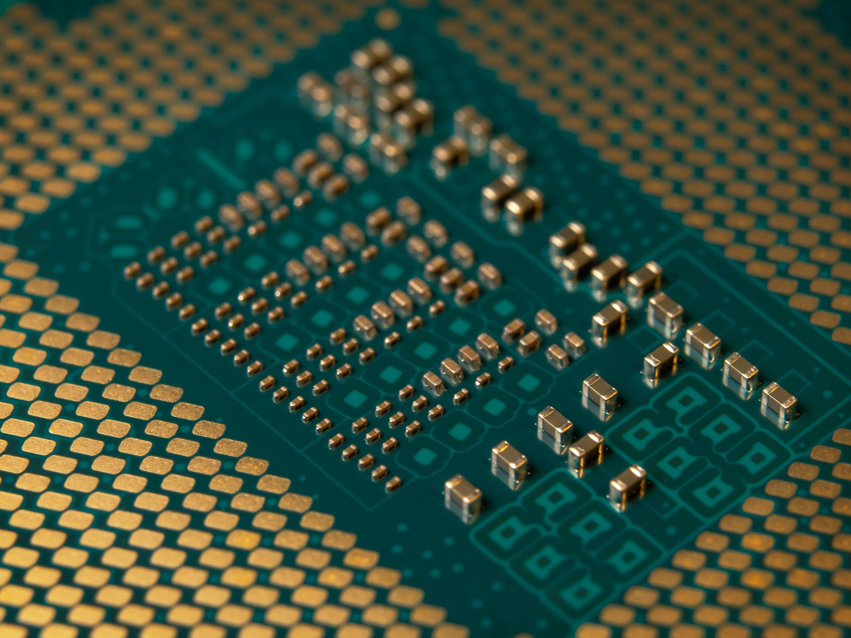
Advanced chip packaging, a term hitherto known only to semiconductor insiders, has ascended to a position of unprecedented importance in the realm of artificial intelligence. The technology, refined by specialists such as Subramanian Iyer at the University of California, Los Angeles, involves the intricate bundling of semiconductor components into palm-sized modules.
This process, while seemingly arcane, has become a linchpin in the race to harness A.I. capabilities. By boosting computational efficiency and power, it enables the processing of complex A.I. algorithms that were once out of reach.
Historically, the semiconductor industry has focused on shrinking the size of transistors to enhance performance. However, as this approach reaches physical limits, advanced chip packaging has emerged as a crucial alternative. By stacking chips vertically and connecting them with high-speed interconnects, this technology effectively multiplies processing power without the need for further miniaturisation.
The implications are profound. With A.I. systems increasingly driving sectors from healthcare to finance, the demand for robust processing capabilities has never been higher. The United States, keen to maintain its edge in A.I., finds itself reliant on this niche technology, creating a strategic chokepoint in the global tech race.
Yet, the path forward is fraught with challenges. The complexity of manufacturing these advanced packages requires significant investment in research and development. Moreover, geopolitical tensions exacerbate supply chain vulnerabilities, with countries vying for dominance in semiconductor technology.
In this high-stakes environment, the field of advanced chip packaging is no longer a quiet backwater of the tech world. It is at the cutting edge of a global contest for A.I. supremacy, shaping the future of technology in ways few could have predicted.